PMIC PV Compensation Configuration in Preboot Guide
This document provides a guide for configuring the Power Management Integrated Circuit (PMIC) in the VSSDK environment. This guide only supports SL16xx chips. The PMIC configuration defines how the system regulates CORE and CPU voltages during Preboot.
Audience: Customers and integrators who need to configure PMIC behavior in Preboot without modifying source code.
PMIC mode selection
The first step is to select the PMIC control interface supported by the hardware design. In the product defconfig, enable one of the following modes.
Macro |
Description |
|---|---|
CONFIG_PMIC_IF_I2C=y |
Controls the PMIC through the I2C bus using model-specific drivers. |
CONFIG_PMIC_IF_PWM=y |
Controls regulator voltage through PWM duty cycle. |
└─CON FIG_PMIC_PWM_BACKEND_SMTIMER=y |
For PWM mode, uses the SM Timer block to generate PWM. |
└ ─CONFIG_PMIC_PWM_BACKEND_PWM=y |
For PWM mode, uses the SOC PWM controller, also referred to as Typical PWM. |
CONFIG_PMIC_IF_AUTO=y |
Auto-detection mode. Identifies several possible I2C PMICs based on GPIO strap pins. |
Detailed configuration modes
I2C PMIC mode
Use this mode when the PMIC is regulated through I2C commands, for example tps62868 or sy8827n.
Key parameters
CONFIG_VCORE_PMIC_MODEL: Model name of the PMIC supplying VCORE. It must match an entry in pmic_models. Here is the candidate PMICs:
( ) None
( ) m88pg86x
( ) sy8824b
( ) ncp6335d
( ) mp886x
( ) sy8827n
( ) hl7593wl06
( ) tps62868
( ) rt5739
( ) pwm_pmic
(X) tps6287x
( ) rt5733
( ) smtimer
CONFIG_VCPU_PMIC_MODEL: Model name for VCPU. This may be empty if VCORE and VCPU share the same rail. Candidate PMICs: same as above.CONFIG_VCORE_PMIC_I2CCH: Display name of the I2C bus. Here is the candidate I2C bus:
( ) NONE
( ) TW0
( ) TW1
( ) TW1A
( ) TW1B
(X) TW2
( ) TW2A
( ) TW2B
( ) TW3
( ) TW3A
( ) TW3B
CONFIG_VCORE_PMIC_I2CCH_NUM: Numeric I2C bus index, usually auto-generated from the bus name.
Example
CONFIG_PMIC_IF_I2C=y
CONFIG_VCORE_PMIC_MODEL="tps62868"
CONFIG_VCPU_PMIC_MODEL=""
CONFIG_VCORE_PMIC_I2CCH="TW2"
CONFIG_VCORE_PMIC_I2CCH_NUM=4
PWM PMIC mode
Use this mode when the regulator output voltage is controlled by the duty cycle of a PWM signal.
In PWM PMIC mode, Preboot converts the target voltage into a PWM duty
value by linear interpolation between two calibration points:
(VOLT_MIN_UV, DUTY_AT_VOLT_MIN) and (VOLT_MAX_UV, DUTY_AT_VOLT_MAX).
The PWM signal is typically filtered by an RC low-pass filter and then connected into the buck regulator feedback network. Because of this, the voltage-to-duty relationship is board-specific and depends on the schematic, resistor values, PWM polarity, and component tolerances.
PWM backend selection
When CONFIG_PMIC_IF_PWM=y is selected, one PWM backend must also be
selected.
Backend macro |
Description |
Co ntroller clock |
|---|---|---|
|
Uses the SOC PWM controller, also referred to as Typical PWM. |
100 MHz |
|
Uses the SM Timer block in PWM mode. |
25 MHz |
PWM controller clock and output frequency
For SL1680, SL1640, and SL1620, the PWM controller clock frequencies are as follows.
Chip |
SOC PWM controller clock |
SM Timer PWM clock |
|---|---|---|
SL1680 |
100 MHz |
25 MHz |
SL1640 |
100 MHz |
25 MHz |
SL1620 |
100 MHz |
–(No SM Timer PWM in SL1620) |
Note
Important: These are the input clocks of the PWM generators, not the final PWM output frequency seen on the pin.
The actual PWM output frequency is configured by
CONFIG_VCORE_PWM_FREQ_HZ and CONFIG_VCPU_PWM_FREQ_HZ.
SOC PWM:
    controller clock = 100 MHz
    CONFIG_VCORE_PWM_FREQ_HZ = 100000 (typical PWM output frequency = 100kHz)
    terminal count = 100000000 / 100000 = 1000

SM Timer PWM:
    controller clock = 25 MHz
    CONFIG_VCORE_PWM_FREQ_HZ = 100000 (typical PWM output frequency = 100kHz)
    terminal count = 25000000 / 100000 = 250
    actual PWM output frequency = 100 kHz
Both backends can generate the same output frequency, but their duty-cycle resolution is different because their controller clocks are different.
Backend |
Controller clock |
Terminal count at 100 kHz |
Duty resolution |
|---|---|---|---|
SOC PWM |
100 MHz |
1000 |
1 / 1000 |
SM Timer PWM |
25 MHz |
250 |
1 / 250 |
Note
Recommendation: For regulator control, SOC PWM is preferred when available because it provides better duty-cycle resolution. SM Timer PWM should be used only when the board routes the regulator control signal to an SM Timer output pin.
Key parameters
Parameter |
Description |
|---|---|
|
GPIO pin number used for the VCORE PWM signal. |
|
GPIO pin number used for the VCPU PWM signal. Leave empty or set to none if unused. |
|
Desired PWM output frequency in Hertz. A typical value is 100000 for 100 kHz. |
|
Desired PWM output frequency in Hertz. A typical value is 100000 for 100 kHz. |
|
PWM polarity for VCORE. 0 means normal or non-inverted. 1 means inverted. |
|
PWM polarity for VCPU. 0 means normal or non-inverted. 1 means inverted. |
|
Minimum VCORE output voltage in microvolts. |
|
Maximum VCORE output voltage in microvolts. |
|
Minimum VCPU output voltage in microvolts. |
|
Maximum VCPU output voltage in microvolts. |
|
Duty value corresponding to
|
|
Duty value corresponding to
|
|
Duty value corresponding to
|
|
Duty value corresponding to
|
CONFIG_*_PWM_GPIO Configuration Rules:
Since a PWM channel can be mapped to different pads, the unique GPIO number identifies the pin connected to the PMIC PWM signal and determines the PWM channel configuration. Refer to the board schematic and PMIC datasheet for the PWM GPIO connection.
- SoC GPIO:
    Enter the GPIO number directly.

- SM GPIO:
    Set bit[31:30] to 2'b10 and place the SM GPIO number
    in bits[29:0].

- GPIO-X:
    Set bit[31:30] to 2'b01 and place the GPIO_X number
    in bits[29:0].

Examples:
SoC GPIO 15:
    0xf

SM GPIO 3:
    0x80000003


GPIO_X10:
    0x4000000A
Note
Matched parameters: PWM_POLARITY, DUTY_AT_VOLT_MIN, and
DUTY_AT_VOLT_MAX must be treated as a matched set. If polarity changes,
both duty endpoints must be re-measured. Besides, the duty endpoints
must be measured and should be matched to VOLT_MIN_UV and VOLT_MAX_UV
Example
SL1620 SBC board with only one VCORE power rail
PMIC Control Interface (PWM) --->
PWM Backend (PWM Controller) --->
(0x2b) GPIO used to identify VCORE TYPICAL PWM PIN
(0xff) GPIO used to identify VCPU TYPICAL PWM PIN
(100000) VCORE PWM Frequency (Hz)
(0) VCORE PWM Polarity
(700000) VCORE PWM Voltage Min (uV)
(990000) VCORE PWM Voltage Max (uV)
(958) VCORE PWM Duty Cycle at Volt Min
(0) VCORE PWM Duty Cycle at Volt Max
(100000) VCPU PWM Frequency (Hz)
(0) VCPU PWM Polarity
(700000) VCPU PWM Voltage Min (uV)
(990000) VCPU PWM Voltage Max (uV)
(958) VCPU PWM Duty Cycle at Volt Min
(0) VCPU PWM Duty Cycle at Volt Max
SM Timer PWM mode
SM Timer PWM mode is a backend of PWM PMIC mode. It uses the SM Timer block to generate a PWM waveform.
Use this backend only when the board routes the PMIC control signal to an SM Timer output pin.
CONFIG_PMIC_IF_PWM=y
CONFIG_PMIC_PWM_BACKEND_SMTIMER=y
For SL1680 and SL1640, the SM Timer PWM controller clock is 25 MHz. SL1620 has no SM Timer PWM controller.
The PWM output frequency is still configured by CONFIG_VCORE_PWM_FREQ_HZ
and CONFIG_VCPU_PWM_FREQ_HZ.
CONFIG_VCORE_PWM_FREQ_HZ = 100000

SM Timer terminal count:
    25000000 / 100000 = 250

PWM output frequency:
    25 MHz / 250 = 100 kHz
Compared with SOC PWM, SM Timer PWM has lower duty resolution at the same output frequency.
SOC PWM at 100 kHz:
    100 MHz / 100 kHz = 1000 steps

SM Timer PWM at 100 kHz:
    25 MHz / 100 kHz = 250 steps
Note
Recommendation: If both routing options are available, SOC PWM is recommended for PMIC voltage control.
The remaining voltage, duty, and polarity parameters are the same as in the PWM PMIC mode section above.
Example
Example board configuration:
PMIC Control Interface (PWM) --->
PWM Backend (SM Timer Controller) --->
(100000) VCORE PWM Frequency (Hz)
(0) VCORE PWM Polarity
(780000) VCORE PWM Voltage Min (uV)
(1000000) VCORE PWM Voltage Max (uV)
(250) VCORE PWM Duty Cycle at Volt Min
(0) VCORE PWM Duty Cycle at Volt Max
(100000) VCPU PWM Frequency (Hz)
(0) VCPU PWM Polarity
(791000) VCPU PWM Voltage Min (uV)
(1000000) VCPU PWM Voltage Max (uV)
(250) VCPU PWM Duty Cycle at Volt Min
(5) VCPU PWM Duty Cycle at Volt Max
(0x8000000E) GPIO used to identify VCORE SMTIMER PWM PIN
(0x8000000F) GPIO used to identify VCPU SMTIMER PWM PIN
Auto-detection mode (only support I2C PMIC models)
Use this mode when a single PCB design may be populated with different PMIC models. The system reads two GPIO pins to determine which PMIC model is present.
GPIO state mapping
GPIO_H=0, GPIO_L=0→ Model 0GPIO_H=0, GPIO_L=1→ Model 1GPIO_H=1, GPIO_L=0→ Model 2GPIO_H=1, GPIO_L=1→ Model 3
Key parameters
CONFIG_VCORE_PMIC_GPIOH: GPIO index for the high-bit strap. The configuration rule refers toCONFIG\_*_PWM_GPIOConfiguration Rules.CONFIG_VCORE_PMIC_GPIOL: GPIO index for the low-bit strap. Same configuration rule as above.CONFIG_VCORE_PMIC_MODEL_0toCONFIG_VCORE_PMIC_MODEL_3: Model names for each strap combination. Fill in these parameters for the supported PMIC models:
m88pg86x,sy8824b,ncp6335d,mp886x,sy8827n,hl7593wl06,tps62868,rt5739,tps6287x,rt5733
Example
CONFIG_PMIC_IF_AUTO=y
CONFIG_VCORE_PMIC_GPIOH=0xA
CONFIG_VCORE_PMIC_GPIOL=0xB
CONFIG_VCORE_PMIC_MODEL_0="tps62868"
CONFIG_VCORE_PMIC_MODEL_1="sy8827n"
CONFIG_VCORE_PMIC_MODEL_2="none"
CONFIG_VCORE_PMIC_MODEL_3="none"
CONFIG_VCORE_PMIC_I2CCH="TW2"
CONFIG_VCORE_PMIC_I2CCH_NUM=4
How to apply and verify
Applying configuration
Begin modifying the configuration recipe:
devtool modify synasdk-config-native
Edit the product
defconfigfile, for examplebuild-sl2619/workspace/sources/synasdk-config-native/configs/product/sl2619_poky_aarch64_rdk/sl2619_poky_aarch64_rdk_defconfig.Run the configuration command.
devtool build synasdk-config-native
Building
Trigger a rebuild of the Preboot components.
devtool build synasdk-preboot
Run devtool build-image astra-media to build the complete image containing this change.
Verification
Check the build log for the following indicators.
I2C success: messages indicating PMIC configuration binary generation for I2C mode completed successfully.
PWM success: messages indicating PMIC configuration binary generation for PWM mode, including configured PWM frequency values.
Artifact check: confirm that
build-sl2619/tmp/work/sl2619-poky-linux/synasdk-preboot/scarthgap_6.12_v2.4.0+git/synasdk-preboot-scarthgap_6.12_v2.5.0+git/target/preboot/intermediate/release/pmic_config.binhas been generated.
Best practices and troubleshooting
Avoid parameter misalignment: If an error such as Unknown option ‘1’ appears, ensure optional parameters are not left in an unexpected empty state. Use default values where appropriate.
Number base: Pay attention to whether each value should be entered in hexadecimal or decimal format. Check the corresponding help text before configuring the value.
Voltage units: Always use microvolts for voltage settings. For example, 0.9 V must be written as
900000.VCPU versus VCORE: If the board uses a shared rail for both VCORE and VCPU, leave the VCPU-specific fields empty or keep them same with VCORE or just keep the default value.
Consistency with Linux: If Linux later controls the same PWM regulator, keep PWM polarity, frequency, and duty mapping consistent with the Linux device tree to avoid voltage glitches during handoff.
Test on board
The boot log may appear as shown below, and use a digital multimeter to measure the corresponding voltage.
set Vcpu from XXXuv to XXXuv
or
set Vcore from XXXuv to XXXuv
or
Vcore is XXXuV, default setting by hardware.
or
Vcpu is XXXuV, default setting by hardware.
or
skip vcpu pv_comp !!!!
To clearly observe the voltage changes, follow the steps below:
Boot into the Linux kernel and set the CPU voltage to the highest level.
MAX=$(cat /sys/devices/system/cpu/cpu0/cpufreq/cpuinfo_max_freq)
echo $MAX > /sys/devices/system/cpu/cpu0/cpufreq/scaling_min_freq
b. Reboot the system. During boot, the boot log will show the CPU voltage changing from the highest default voltage to the voltage determined by the leakage ID. Use a digital multimeter to measure the voltage at the corresponding stages.
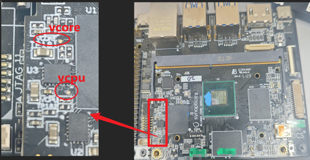
The voltage measurement point is illustrated in the figure below. On the SL1680 RDK board, the silkscreen marking is located in the red rectangle. The same silkscreen marking can also be found on SL1640 and SL1620.
Quick reference
Topic |
Value |
|---|---|
SOC PWM controller clock on SL1680 / SL1640 / SL1620 |
100 MHz |
SM Timer PWM controller clock on SL1680 / SL1640 |
25 MHz |
Typical recommended PWM output frequency |
100 kHz |