SL2600 User Guide
Introduction
The Synaptics Astra™ Machina SL2600 Series Developer Kit enables easy and rapid prototyping of multimodal AI-native IoT applications. A flexible design approach supports a core compute module, an I/O base board, daughter cards for integrated Wi-Fi / Bluetooth connectivity, debug, and programmable I/O. The evaluation system supports the Synaptics SL2619 SoC family that delivers unprecedented levels of price performance for the IoT, and enabled via an open, unified software experience built on Yocto Linux. The Machina SL2600 Series is powered by the open-source Synaptics Torq™ Edge AI platform, leveraging the Torq T1 and the Coral NPU subsystems.
Scope
This user guide describes the hardware configuration and functional details for the Astra Machina SL2610 core module, I/O board, and supported daughter cards, in addition to the bring-up sequence for the developer kit.
Definition of Board Components
Astra Machina: Combined system with core module, I/O board, and supported daughter cards.
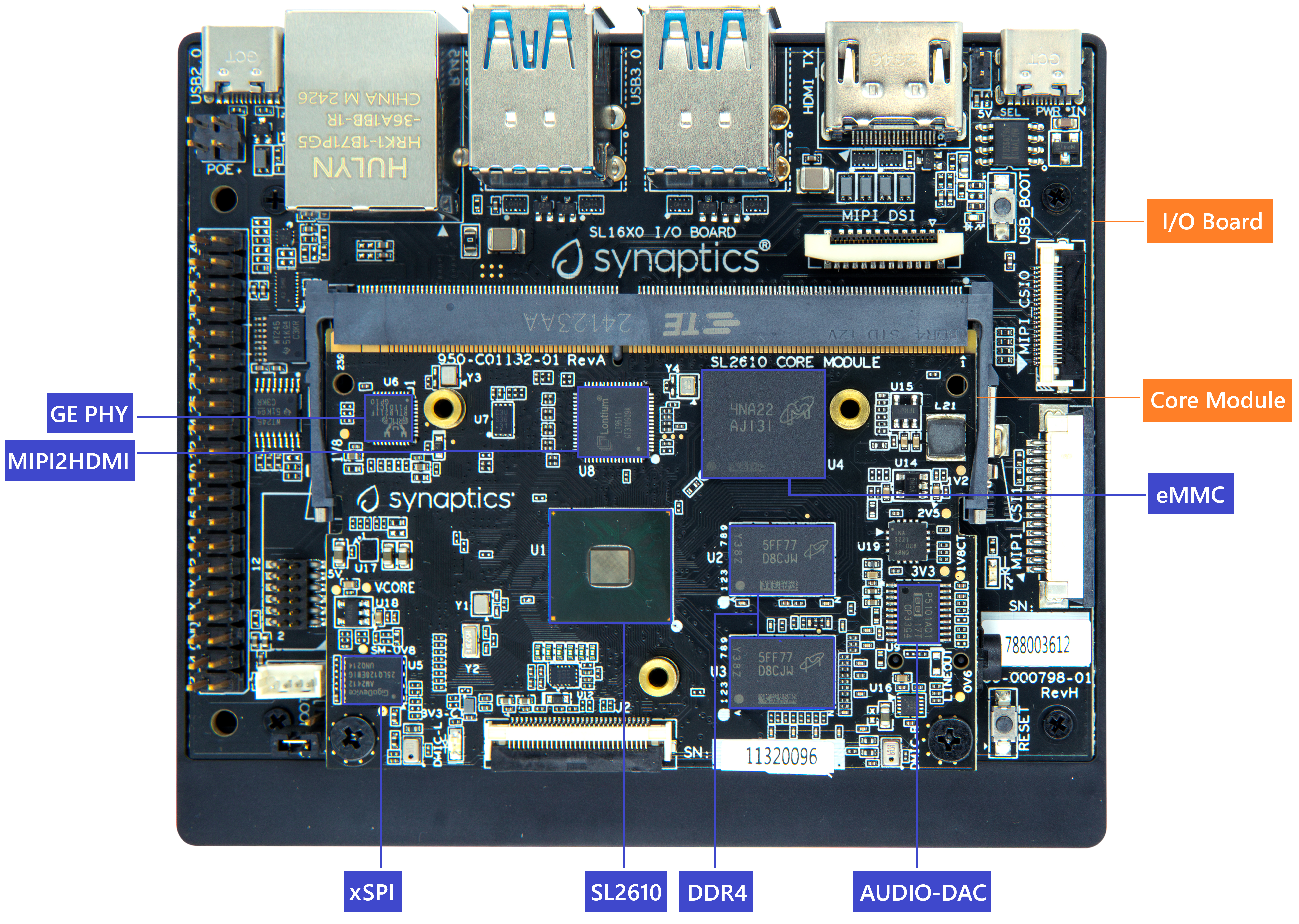
Core module: Processor subsystem module with key components including SL2610, eMMC, and DDR4.
I/O board: Common base board that includes various standard hardware interfaces, buttons, headers, and power-in.
Daughter card: Add-on boards for supporting various features such as connectivity, debug, and other flexible I/O options.
Astra Machina System Overview
This section covers system features, block diagrams and top views of the Astra Machina developer kit.
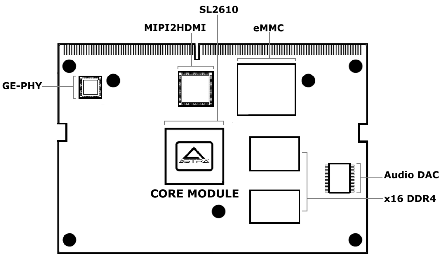
SL2610 Core Module (Dimensions: W x H = 69.6 mm x 47.38 mm)
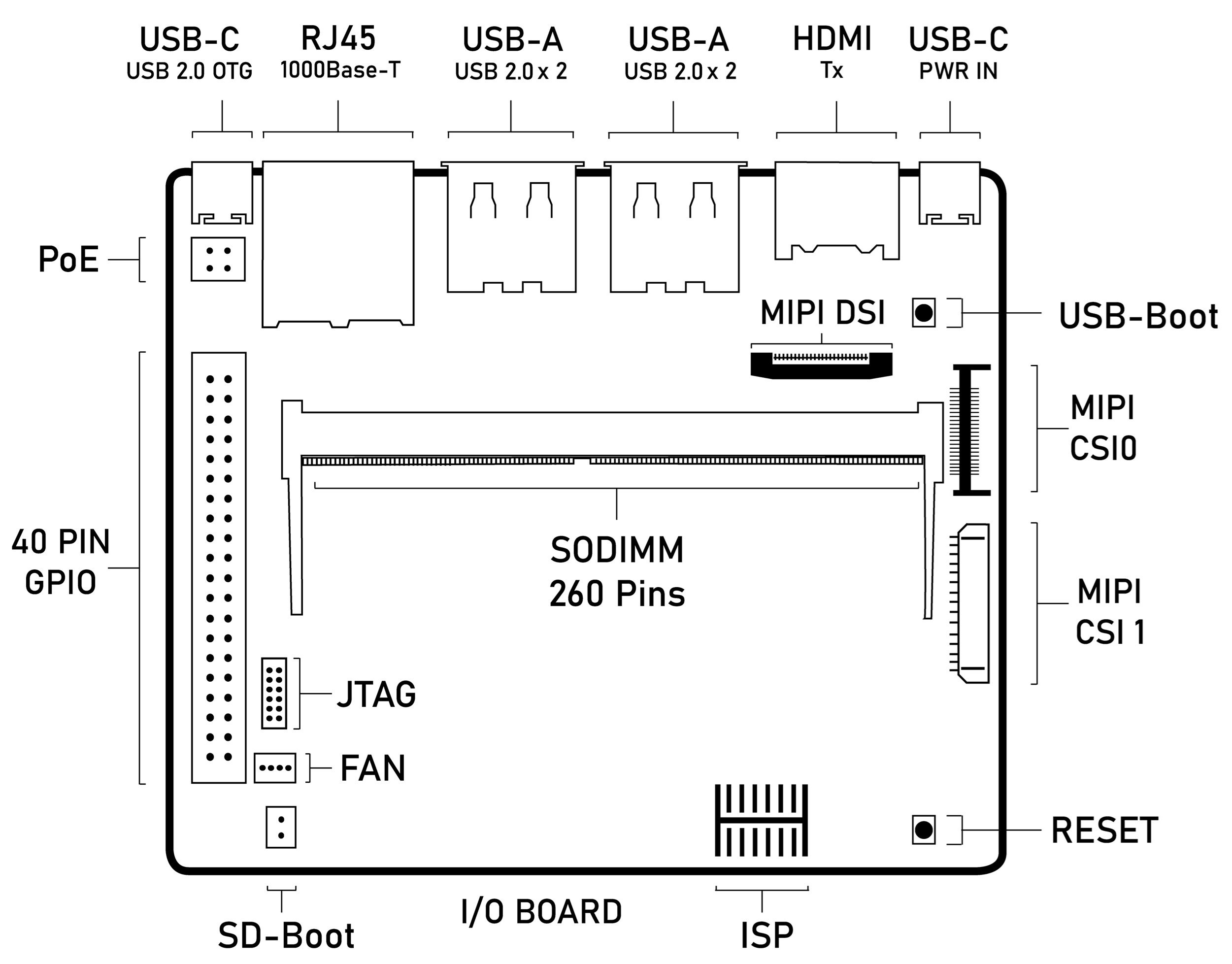
I/O Board
Features
The SL2610-based developer kit includes the following components:
Main components on the core module:
Synaptics SL2610 Dual-Core Arm® Cortex®-A55 embedded IoT processor, up to 2.0 GHz
Storage: eMMC 5.1 (32 GB [1]_)
DRAM: up to x16 4GB system memory by 2pcs x8 16Gbit DDR4
PMIC: support DVFS in Vcore supply rail
MIPI DSI to HDMI 1.4 output
SD Card Receptacle
Line-out: direct Line Level 2.1-VRMS stereo output
DMIC: 2 digital microphones – 1 PDM stereo audio input
Main components on the I/O board:
M.2 E-key 2230 Receptacle: It supports SDIO, UART for Wi-Fi/BT modules
USB 2.0 Type-A: 4 ports to support host mode at Hi-Speed.
USB 2.0 Type-C: supports OTG host or peripheral mode at Hi-Speed.
Push buttons: used for USB-BOOT selection and system RESET.
2pin Header: used for SD-BOOT selection.
Daughter card interface options:
MIPI DSI on 22-pin FPC interface to support 4-lane DSI plus I2C and GPIOs for up to 1080p60 display panel.
MIPI CSI on 22-pin at CSI0 for 2-lane plus I2C and GPIOs, for up to 2160p30 resolution.
JTAG daughter card for debug.
40-pin header for additional functions
4-pin PoE+ connector, with a PoE hat board (purchased separately), it offers an add-on voltage regulator module for PoE+ Type2 (802.3at) power device. Available power shall be 25.5W (Class 4) at 5V pins of 40-pin header to I/O board.
Type-C power supply with 15V @ 1.8A.
SL2610 System Block Diagram
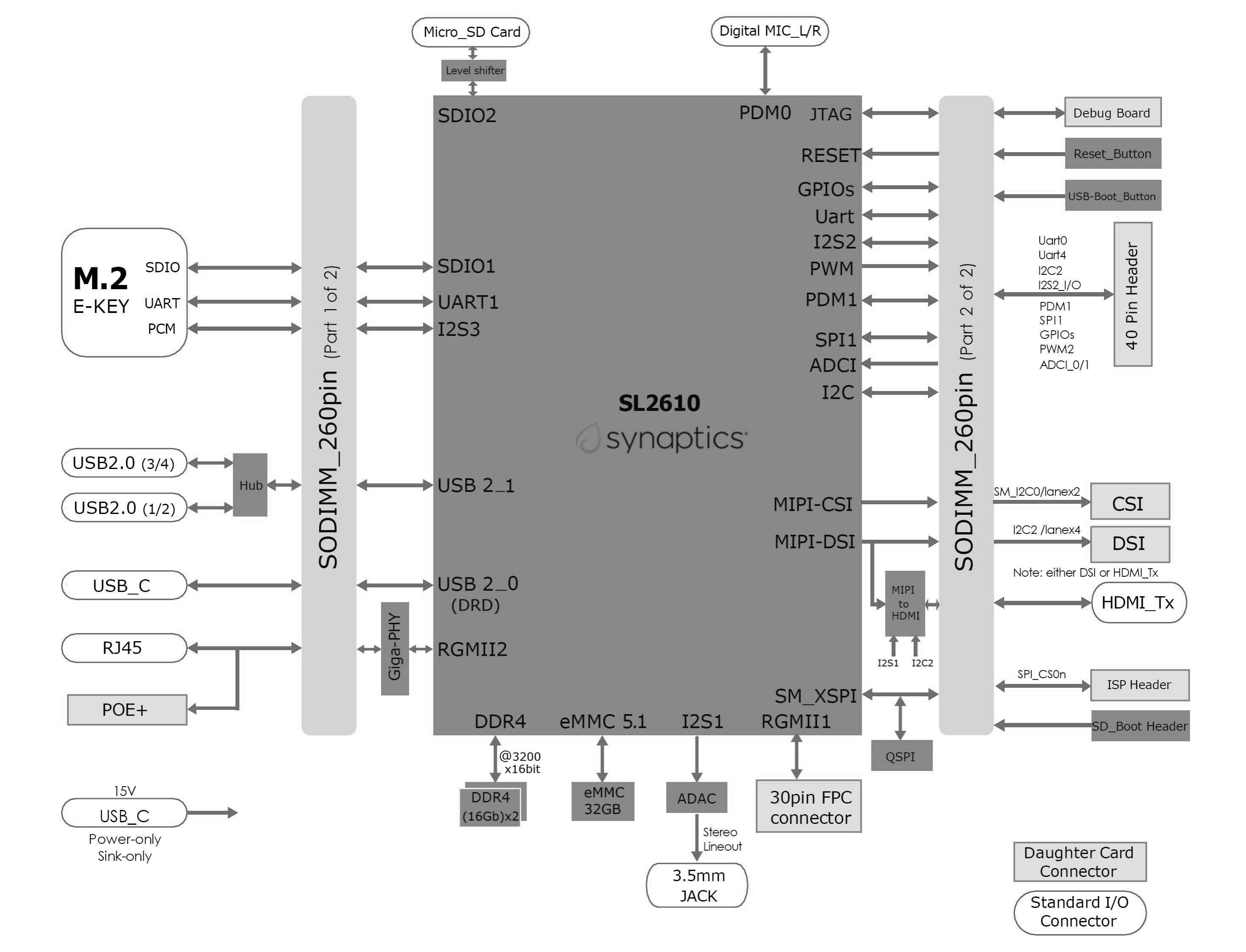
SL2610 System Block Diagram
Top view of SL2610 Astra Machina developer kit
Top view of SL2610 Developer Kit
System connectors
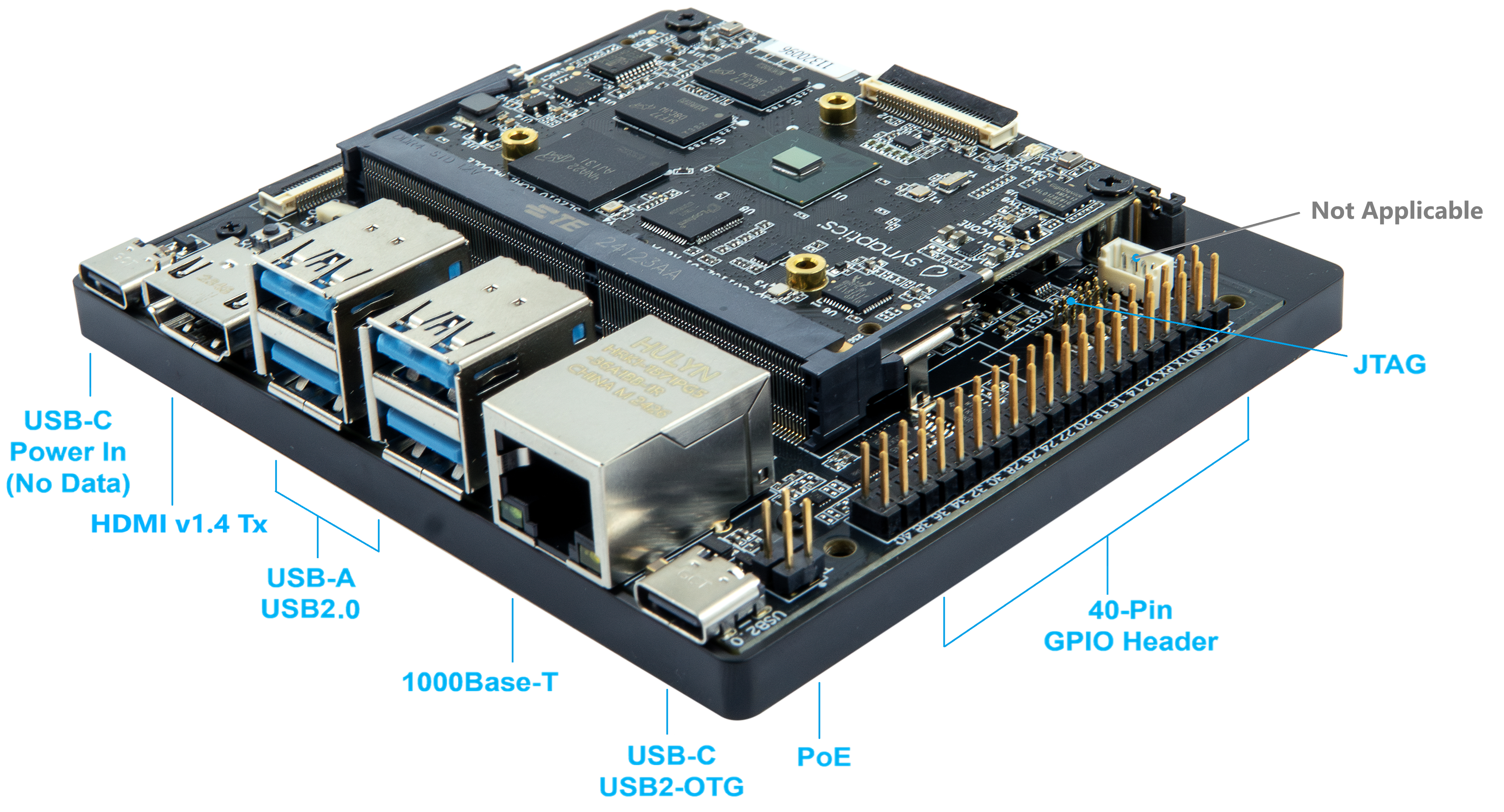
Front View
Rear View
Astra Machina Board Control/Status & System I/O
This section covers boot-up, LEDs status indicators, buttons, connectors, and pin-strap settings.
Booting Up
The Astra Machina supports booting from three interfaces. Users can select a boot interface before powering up, as follows:
eMMC boot: Default boot interface.
SD boot: Short SD_Boot header by 2.54mm jumper-cap before power-up, see SD_Boot header in Locations of jumper on I/O board. Ensure SD-Card with firmware is plugged into SD-slot on core module in Locations on core module bottom side.
USB boot: Connect USB-C USB2.0 port to the host PC, then follow the procedure in Hardware Manual Button Settings.
LEDs
LED locations
LED locations on I/O board shows the LED locations on the I/O board.
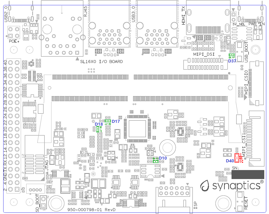
LED locations on I/O board
LED definitions
LED |
Color |
LEDs Function |
|---|---|---|
D10 |
Green |
LED indicator for USB3.0 Hub is working in normal mode or suspend mode. |
D17 |
Green |
LED indicator1 for M.2 device general purpose. |
D18 |
Green |
LED indicator2 for M.2 device general purpose. |
D37 |
Green |
LED indicator for Power-on status. |
D40 |
RED |
LED indicator for Stand-By Status. |
SM PinStrap and Boot-up Settings
Pin# |
Pin Mux Name |
Setting Value Default* |
Resistor Stuffing
|
Description Rpu = OnChip Pull-up Rpd = OnChip Pull-down |
|---|---|---|---|---|
N30 |
PLLBYPS |
— |
— |
Straps for CPU reset bypass |
0* |
-R190 |
0: Enable reset logic inside CPU partition |
||
1 |
+R190 |
1: Bypass reset logic inside CPU partition |
||
B24 |
dft_jtag_sel |
— |
— |
Straps for JTAG_SEL |
0* |
-R31 |
0: ATE/RMA mode — Functional JTAG is selected |
||
1 |
+R31 |
1: ATE/RMA mode — DFT JTAG is selected |
SoC PinStrap and Boot-up Settings
Pin# |
Pin Mux Name |
Setting Value Default* |
Resistor Stuffing
|
Description Rpu = OnChip Pull-up Rpd = OnChip Pull-down |
|---|---|---|---|---|
C5 |
CPURSTBYPS |
— |
— |
Straps for CPU reset bypass |
0* |
— |
0: Enable reset logic inside CPU partition |
||
1 |
— |
1: Bypass reset logic inside CPU partition |
||
B13 |
SOFTWARE_STRAP[0] |
— |
— |
Straps for software usage (Rpu) |
0 |
+R34 |
Version control for Core-Module Rev B |
||
1* |
-R34 |
Version control for Core-Module Rev A |
||
AF27 |
SOFTWARE_STRAP[1] |
— |
— |
Straps for software usage (Rpd) |
0* |
-R35 |
Default setting |
||
1 |
+R35 |
Alternate setting |
||
C8 |
SOFTWARE_STRAP[2] |
— |
— |
Straps for software usage (Rpd) |
0* |
-R36 |
Default setting |
||
1 |
+R36 |
Alternate setting |
||
B9 |
SOFTWARE_STRAP[3] |
— |
— |
Straps for software usage (Rpd) |
0* |
-R37 |
Default setting |
||
1 |
+R37 |
Alternate setting |
Net Name |
Strap Name |
Setting Value Default* |
Resistor Stuffing
|
Description Rpu = On-Chip Pull-up Rpd = On-Chip Pull-down |
|---|---|---|---|---|
USB_BOOTn |
USB-Boot |
— |
— |
ROM code uses this strap to determine if booting from USB or not (Rpu). |
0 |
— |
0: Boot from USB when the USB-BOOT button is pressed while system reset is de-asserted. |
||
1* |
— |
1: Boot from the device selected by boot_src[1]. |
||
CONN-SPI.VDIO1P8. BOOT_SRC1 |
SD-Boot |
— |
— |
ROM code uses this strap to determine if booting from SD Card or not (Rpu). |
0 |
— |
0: Boot from SD Card when SD_Boot header is ON while system reset is de-asserted. |
||
1* |
— |
1: Boot from the device selected by boot_src[1] when SD_Boot header is OFF. |
Hardware Manual Button Settings
Switch Block |
Type |
Setting |
Function |
|---|---|---|---|
SW6 (RESET) |
Momentary Pushbutton |
Push |
SL2610 Reset Key asserted |
Release |
Key de-asserted |
||
SW7 (USB_BOOT) |
Momentary Pushbutton |
Push |
USB boot Key asserted. USB-Boot mode requires a combination of the USB_BOOT key and the RESET button. Refer to the steps below for the detailed entry procedure. |
Release |
Key de-asserted |
To enter USB-Boot mode, follow these steps:
Note
Prior to these steps, make sure the USB driver is installed successfully on the PC host side. For details, please reference Astra Yocto Linux User Guide.
Push RESET button to assert system reset to SL2610.
Keep pushing RESET button and push USB_BOOT button at the same time for 1-2 seconds.
Release RESET button while holding USB_BOOT button, so SL2610 enters USB-Boot mode.
Check and wait for the console print… messages.
Once the console print is returned and entered USB boot successfully, release USB_BOOT button.
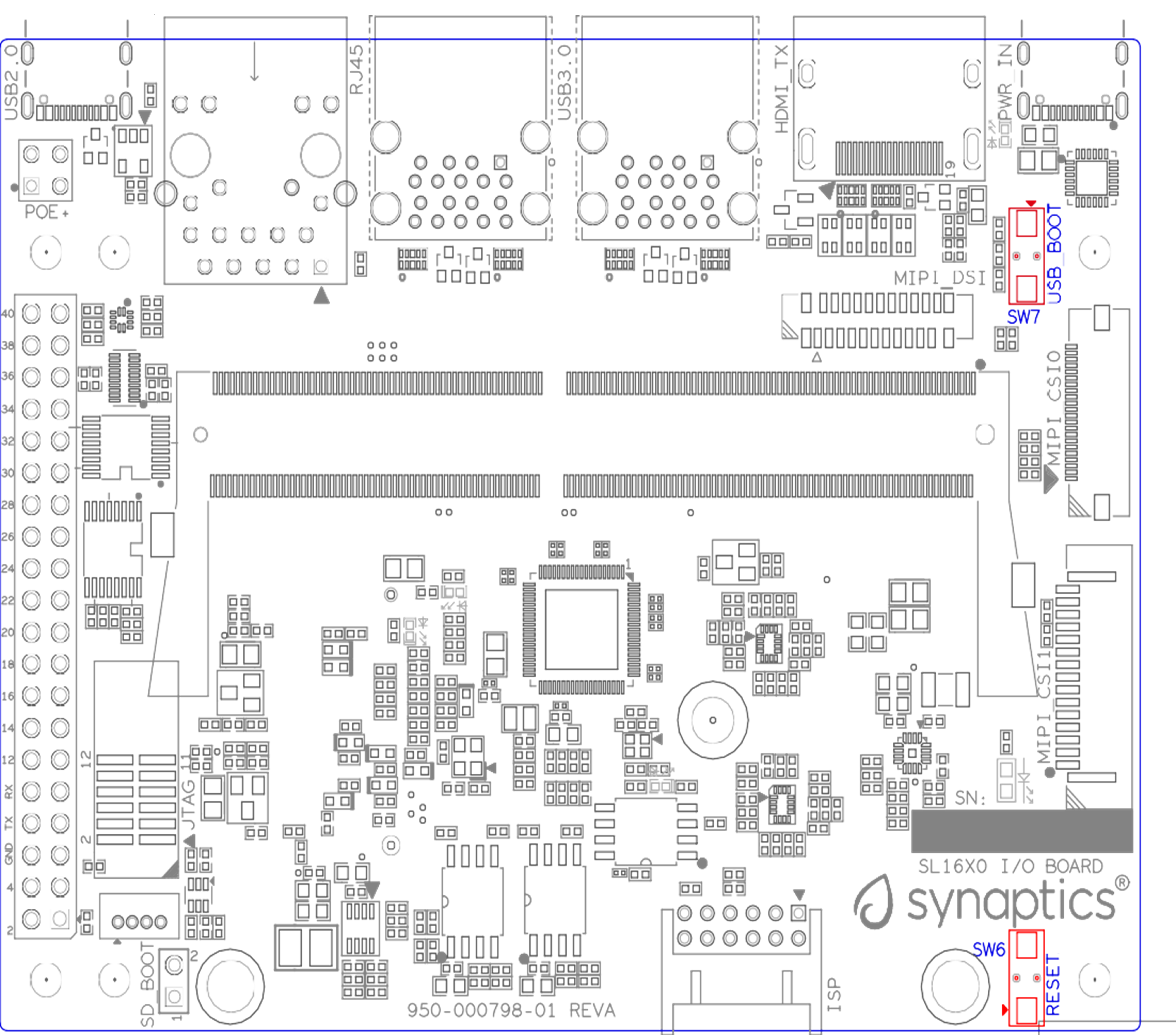
Locations of manual buttons on I/O board
Hardware Jumper Settings
Ref Des |
Type |
Pin Conn ection |
Description |
|---|---|---|---|
JP1 |
2x1 2.54mm header |
1-2 |
SD_Boot selection |
|
|||
|
|||
JP2 |
2x1 2mm header |
1-2 |
5V_SEL selection |
|
|||
|
To enter SD-Boot mode, follow these steps:
Note
Prior to these steps, make sure SD-Card with firmware is plugged into SD-slot on the core module.
Short SD_Boot header by 2.54mm jumper-cap before power-up.
Power-up system, then boot-up from SD_Card.
Locations of jumper on I/O board shows the Header locations on the I/O board.
Locations of jumper on I/O board
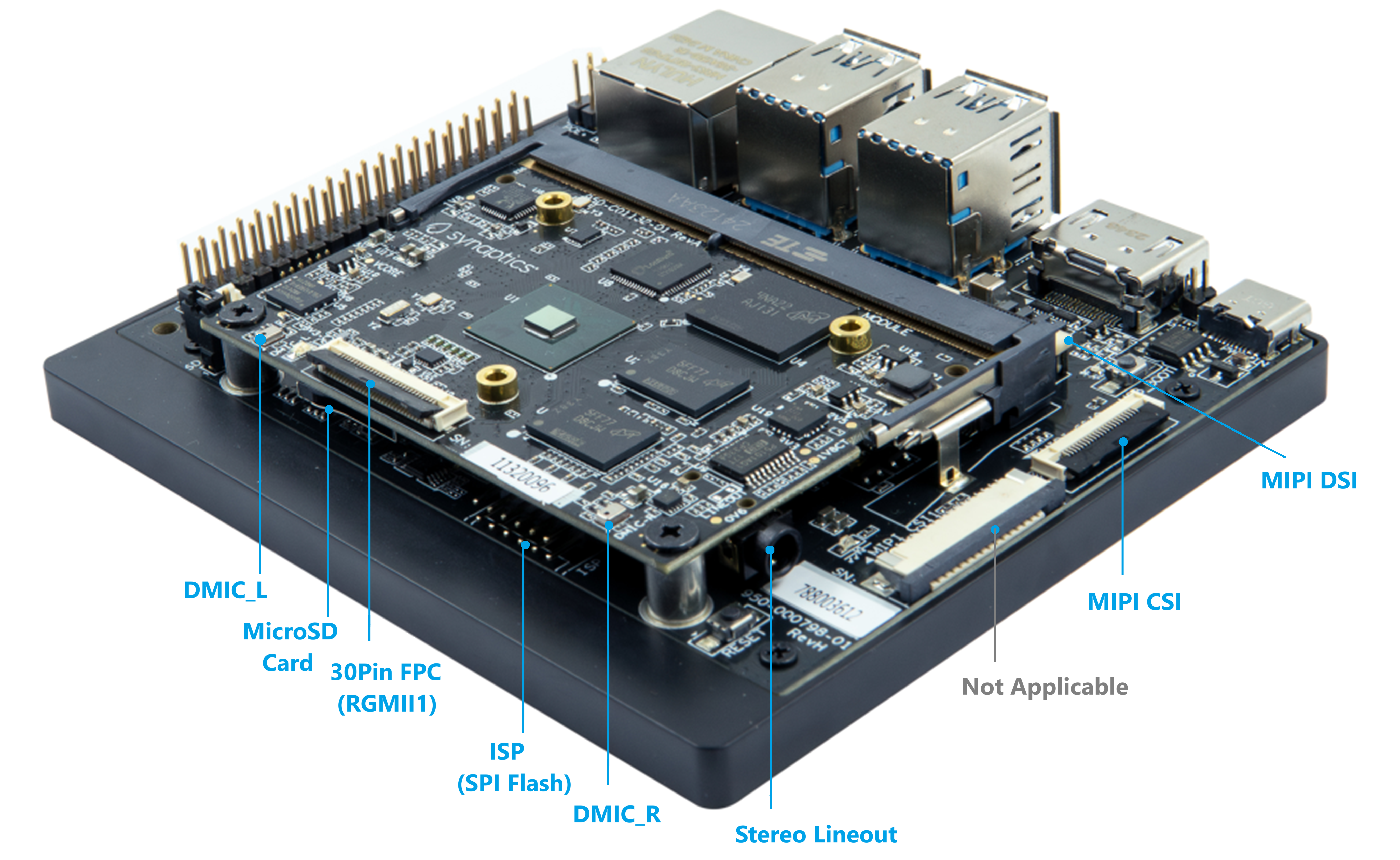
SL2610 Developer Kit Connectors
Locations of core module connectors on top side
Locations on core module top side
Locations of core module connectors on bottom side
Locations on core module bottom side
Core module connector definitions
M ain Ref Des |
Connecting Boar ds/Devices (Ref Des if any) |
F unctions |
Remarks |
|---|---|---|---|
J1 |
Stereo Line out |
Analog audio L/R |
Audio L/R output to 3.5mm Jack. |
J2 |
RGMII1 |
RGMII1 |
Connector for RGMII1 signals through 30-pin FPC cable. |
J3 |
MicroSD Card |
SDIO card |
For microSD type of memory card extension. |
Locations of I/O board connectors on top side
Locations on I/O board top side
Locations of I/O board connectors on bottom side
Locations on I/O board bottom side
I/O board connector definitions
M ain Ref Des |
Connecting Boa rds/Devices (Ref Des if any) |
Functions |
Remarks |
|---|---|---|---|
J1 |
ISP D/C |
SPI |
12-pin daughter card to support offline program SPI NOR flash on core module |
J2 |
RJ45 cable |
Giga Ethernet |
For Wired Ethernet connection |
J12 |
HDMI Sink |
HDMI TX |
For off-board HDMI Sink device connection |
J13 |
FAN |
Heat Dissipation w/ FAN |
Not Applicable for SL2610 |
J17 |
M.2 2230 D/C |
SDIO and PCIe |
1x1/2x2 WiFi/Bluetooth card via SDIO PCIe is not applicable for SL2610. |
J22 |
Debug Board |
JTAG |
XDB debugger for debugging |
J32 |
40-pins Header |
UART, I2C, SPI, PDM, I2SI, GPIOs, STS1, PWM, ADC |
Flexible for support various D/C |
J34 |
PoE+ D/C |
PoE+ |
4-pin PoE+ daughter card with supporting an add-on 5V voltage to 40pin Header. |
J 206 |
MIPI-CSI0 adaptor |
MIPI-CSI |
For MIPI-CSI x2 lane extension, like camera |
J 207 |
MIPI-CSI1 adaptor |
MIPI-CSI |
Not Applicable for SL2610 |
J 208 |
MIPI-DSI adaptor |
MIPI-DSI |
For MIPI-DSI x4 lane extension, like panel |
J 210 |
USB Device |
USB2.0 x2 |
For USB2.0 extension in Device mode only |
J 213 |
Type C power source |
Power Supply |
Power for Astra Machina rated at 15V/1.8A |
J 215 |
Dual-Role USB |
USB2.0 OTG |
For USB2.0 extension, in either Host or Device mode |
J 216 |
USB Device |
USB2.0 x2 |
For USB2.0 extension in Device mode only |
Daughter Cards
A set of daughter cards supplements the Astra Machina system with a range of extensible and configurable functionalities including Wi-Fi and Bluetooth connectivity, debug options and general purpose I/O. Details of currently supported daughter cards are described in this section.
Debug Board
Debug Board (Rev5) allows users to communicate with the SL2610 system over JTAG through a Debugger on a PC host. While connecting the Astra Machina and debug board with a 20-pin flat cable, align pin-1 of the 2x10 cable socket at the debug board side with pin-1 of 2x6 header J22 on the developer kit.
UART on the developer kit and the PC host USB are digitally isolated, with no direct conductive path, eliminating ground loop and back-drive issues when either is powered down.
Debug board connectivity for UART and JTAG shows debug board connectivity facilitating UART and JTAG communications.
Debug board connectivity for UART and JTAG
M.2 Card
An M.2 E-Key socket J17 is provided for a variety of modules in the M.2 form factor. Typical applicable modules support Wi-Fi/BT devices with SDIO
Available modules:
Ampak AP12611_M2 with SYN43711 WiFi6E/BT5.3 1x1 over SDIO on M.2 adaptor
260-Pins SODIMM Definition
A 260-Pins SODIMM connector (PN: TE_2309413-1) joins the core module and the I/O board. Table 9 shows the assignment for the 260-Pins.
Assignment |
Pi n# |
260 -Pins S ODIMM |
Pi n# |
Assignment |
|---|---|---|---|---|
VDDM_0V6_VTT_CTL (From IO_Exp) |
2 |
1 |
N/A |
|
XSPI_SDO |
4 |
3 |
SM_CLKOUT |
|
XSPI_SCLK |
6 |
5 |
XSPI_CLKn |
|
VDDM_control (From IO_Exp) |
8 |
7 |
N/A |
|
N/A |
10 |
9 |
N/A |
|
XSPI_SDI |
12 |
11 |
N/A |
|
XSPI_SS0n |
14 |
13 |
N/A |
|
External_Boot_SRC0 |
16 |
15 |
N/A |
|
N/A |
18 |
17 |
N/A |
|
N/A |
20 |
19 |
N/A |
|
ETH1_RST (From IO_Exp) |
22 |
21 |
N/A |
|
SD-CARD_PWR_EN (From IO_Exp) |
24 |
23 |
N/A |
|
GND |
26 |
25 |
N/A |
|
N/A |
28 |
27 |
N/A |
|
N/A |
30 |
29 |
N/A |
|
GND |
32 |
31 |
N/A |
|
N/A |
34 |
33 |
N/A |
|
N/A |
36 |
35 |
N/A |
|
GND |
38 |
37 |
N/A |
|
N/A |
40 |
39 |
N/A |
|
N/A |
42 |
41 |
N/A |
|
GND |
44 |
43 |
N/A |
|
USB2_0_Dn |
46 |
45 |
N/A |
|
USB2_0_Dp |
48 |
47 |
N/A |
|
GND |
50 |
49 |
N/A |
|
N/A |
52 |
51 |
N/A |
|
N/A |
54 |
53 |
GND |
|
GND |
56 |
55 |
N/A |
|
N/A |
58 |
57 |
N/A |
|
N/A |
60 |
59 |
GND |
|
GND |
62 |
61 |
N/A |
|
USB2_1_Dp |
64 |
63 |
N/A |
|
USB2_1_Dn |
66 |
65 |
GND |
|
GND |
68 |
67 |
MIPI_CSI_RD1p |
|
USB2_0_ID |
70 |
69 |
MIPI_CSI_RD1n |
|
USB-C_VBUS |
72 |
71 |
GND |
|
USB-A_VBUS |
74 |
73 |
MIPI_CSI_RD0n |
|
I2S3_BCLK |
76 |
75 |
MIPI_CSI_RD0p |
|
I2S3_DI |
78 |
77 |
GND |
|
I2S3_DO |
80 |
79 |
MIPI_CSI_RCKp |
|
2S3_LRCK |
82 |
81 |
MIPI_CSI_RCKn |
|
I2S2_DI |
84 |
83 |
GND |
|
URT4_RXD |
86 |
85 |
N/A |
|
PDM_DI1 |
88 |
87 |
N/A |
|
GPIO_11 |
90 |
89 |
GND |
|
SM_GPIO27 |
92 |
91 |
N/A |
|
SM_GPIO26 |
94 |
93 |
N/A |
|
SM_GPIO34 |
96 |
95 |
GND |
|
N/A |
98 |
97 |
N/A |
|
N/A |
1 00 |
99 |
N/A |
|
N/A |
1 02 |
1 01 |
GND |
|
I2S2_BCLK |
1 04 |
1 03 |
N/A |
|
EXPANDER_INT_REQn |
1 06 |
1 05 |
N/A |
|
BOOT_SRC1 |
1 08 |
1 07 |
GND |
|
I2S2_DO |
1 10 |
1 09 |
N/A |
|
I2S2_MCLK |
1 12 |
1 11 |
N/A |
|
I2S2_LRCK |
1 14 |
1 13 |
GND |
|
SM_ADCI[0] |
1 16 |
1 15 |
MIPI_DSI_TD0n |
|
SM_ADCI[1] |
1 18 |
1 17 |
MIPI_DSI_TD0p |
|
SM_URT0_TXD |
1 20 |
1 19 |
GND |
|
SM_URT0_RXD |
1 22 |
1 21 |
MIPI_DSI_TD1n |
|
SPI1_SDI |
1 24 |
1 23 |
MIPI_DSI_TD1p |
|
SPI1_SCLK |
1 26 |
1 25 |
GND |
|
SPI1_SDO |
1 28 |
1 27 |
MIPI_DSI_TCKp |
|
SM_GPIO28 |
1 30 |
1 29 |
MIPI_DSI_TCKn |
|
USB2_OCn |
1 32 |
1 31 |
GND |
|
SPI1_SS3n |
1 34 |
1 33 |
MIPI_DSI_TD3n |
|
SM_GPIO25 |
1 36 |
1 35 |
MIPI_DSI_TD3p |
|
SM_TW0_SDA |
1 38 |
1 37 |
GND |
|
SM_TW0_SCL |
1 40 |
1 39 |
MIPI_DSI_TD2p |
|
SM_AUDIO_MUTE@PD |
1 42 |
1 41 |
MIPI_DSI_TD2n |
|
CAMERA_MUTE@PD |
1 44 |
1 43 |
GND |
|
N/A |
1 46 |
1 45 |
GND |
|
N/A |
1 48 |
1 47 |
HDMI_TX_TCKn |
|
N/A |
1 50 |
1 49 |
HDMI_TX_TCKp |
|
HDMITX_HPD |
1 52 |
1 51 |
GND |
|
N/A |
1 54 |
1 53 |
HDMI_TX_TD0n |
|
HDMI_TX_EDDC_SDA |
1 56 |
1 55 |
HDMI_TX_TD0p |
|
HDMI_TX_EDDC_SCL |
1 58 |
1 57 |
GND |
|
LevelTranslator_ENn |
1 60 |
1 59 |
HDMI_TX_TD1n |
|
LT9611-CEC |
1 62 |
1 61 |
HDMI_TX_TD1p |
|
SM_RSTIn@PU |
1 64 |
1 63 |
GND |
|
JTAG_TDO |
1 66 |
1 65 |
HDMI_TX_TD2n |
|
JTAG_TDI & BT-WIFI_wake-up |
1 68 |
1 67 |
HDMI_TX_TD2p |
|
JTAG_TMS & ETH1/2_INT |
1 70 |
1 69 |
GND |
|
N/A |
1 72 |
1 71 |
N/A |
|
N/A |
1 74 |
1 73 |
N/A |
|
URT4_TXD |
1 76 |
1 75 |
GND |
|
SM_TW1_SDA |
1 78 |
1 77 |
HDMI_TX_PWR_EN |
|
SM_TW1_SCL |
1 80 |
1 79 |
JTAG_TCK |
|
TW2_SDA |
1 82 |
1 81 |
SM_GPIO29 |
|
TW2_SCL |
1 84 |
1 83 |
JTAG_TRSTn |
|
SM_URT1_CTSn for M.2 |
1 86 |
1 85 |
GPIO30 |
|
SM_URT1_RTSn for M.2 |
1 88 |
1 87 |
SM_URT1_RXD for M.2 |
|
PWM2 |
1 90 |
1 89 |
GPIO29 |
|
GND |
1 92 |
1 91 |
SM_URT1_TXD for M.2 |
|
PWR_1V8 |
1 94 |
1 93 |
N/A |
|
PWR_1V8 |
1 96 |
1 95 |
SM_ADCI3 |
|
PWR_1V8_CTL |
1 98 |
1 97 |
SM_ADCI4 |
|
PWR_1V8_CTL |
2 00 |
1 99 |
SM_ADCI5 |
|
PWR_3V3_CTL |
2 02 |
2 01 |
SM_ADCI6 |
|
PWR_3V3_CTL |
2 04 |
2 03 |
SM_ADCI7 |
|
GND |
2 06 |
2 05 |
USB_BOOTn |
|
SDIO1_CLK |
2 08 |
2 07 |
MicroSD-CONN_VOL-SEL |
|
GND |
2 10 |
2 09 |
GePH Y_LED1&&STRP[CFG_LDO0] |
|
SDIO1_CMD |
2 12 |
2 11 |
GePH Y_LED2&&STRP[CFG_LDO1] |
|
GND |
2 14 |
2 13 |
GND |
|
SDIO1_D0 |
2 16 |
2 15 |
RJ45_MDIP0 |
|
GND |
2 18 |
2 17 |
RJ45_MDIN0 |
|
SDIO1_D1 |
2 20 |
2 19 |
GND |
|
GND |
2 22 |
2 21 |
RJ45_MDIP1 |
|
SDIO1_D2 |
2 24 |
2 23 |
RJ45_MDIN1 |
|
GND |
2 26 |
2 25 |
GND |
|
SDIO1_D3 |
2 28 |
2 27 |
RJ45_MDIP2 |
|
GND |
2 30 |
2 29 |
RJ45_MDIN2 |
|
PWR_3V3 |
2 32 |
2 31 |
GND |
|
PWR_3V3 |
2 34 |
2 33 |
RJ45_MDIP3 |
|
PWR_3V3 |
2 36 |
2 35 |
RJ45_MDIN3 |
|
PWR_3V3 |
2 38 |
2 37 |
GND |
|
PWR_3V3 |
2 40 |
2 39 |
PWR_BL_5V |
|
PWR_3V3 |
2 42 |
2 41 |
PWR_BL_5V |
|
GND |
2 44 |
2 43 |
GND |
|
GND |
2 46 |
2 45 |
GND |
|
GND |
2 48 |
2 47 |
GND |
|
GND |
2 50 |
2 49 |
GND |
|
PWR_5V |
2 52 |
2 51 |
PWR_5V |
|
PWR_5V |
2 54 |
2 53 |
PWR_5V |
|
PWR_5V |
2 56 |
2 55 |
PWR_5V |
|
PWR_5V |
2 58 |
2 57 |
PWR_5V |
|
PWR_5V |
2 60 |
2 59 |
PWR_5V |
40-Pin Header
A 40-pin GPIO header with 0.1-inch (2.54mm) pin pitch is on the top edge of the I/O board. Any of the general-purpose 3.3V pins can be configured in software with a variety of alternative functions. For more information, please refer to the SL2610 Datasheet.
Note
Pin16/Pin18 are ADCI[0]/[1], the full-scale voltage is 1.8V @ max.
40-Pins header definition
Pin-demuxing for Standard Interface Configuration
This section covers pin-demuxing configuration for the SL2610 developer kit.
For System Manager (SM), see SM Pin-demuxing usage.
For System on Chip (SoC), see SoC Pin-demuxing usage.
SL2610 System Manger (SM) Domain |
|||
|---|---|---|---|
PAD NAME |
Mode Setting |
Default Usage |
Default Function description |
SM_GPIO0 |
OPT2 |
SM_GPIO0 |
ETH_1_INTÐ2_INT |
SM_GPIO1 |
OPT2 |
SM_GPIO1 |
BT_Host_Wake & WiFi_Host_Wake |
SM_GPIO2 |
OPT4 |
I2S2_MCLK |
I2S2_MCLK to 40-PIN |
SM_GPIO3 |
OPT5 |
SM_I3C_MS_SCL |
I2C For PMIC-Vcore DVFS |
SM_GPIO4 |
OPT5 |
SM_I3C_MS_SDA |
I2C For PMIC-Vcore DVFS |
SM_GPIO5 |
OPT1 |
SM_GPIO5 |
VCPU/VCORE_ON# |
SM_GPIO6 |
OPT2 |
SM_SPI1_SS3n |
SM_SPI1_SS3n to 40-PIN |
SM_GPIO7 |
OPT2 |
SM_URT0_RXD |
SM_URT0_RXD to 40-PIN |
SM_GPIO8 |
OPT2 |
SM_URT0_TXD |
SM_URT0_TXD to 40-PIN |
SM_GPIO9 |
OPT3 |
SM_SPI1S_SDO |
SM_SPI1_SDO to 40-PIN |
S M_GPIO10 |
OPT3 |
SM_SPI1S_SCLK |
SM_SPI1_SCLK to 40-PIN |
S M_GPIO11 |
OPT3 |
SM_SPI1S_SDI |
SM_SPI1_SDI to 40-PIN |
S M_GPIO12 |
OPT2 |
SM_TW0_SCL |
Power Sensor + IO exp + MIPI_CSI0 |
S M_GPIO13 |
OPT2 |
SM_TW0_SDA |
Power Sensor + IO exp + MIPI_CSI0 |
S M_GPIO14 |
OPT7 |
SM_URT1_CTSn |
SM_UART1 to WIFI/BT Module |
S M_GPIO15 |
OPT7 |
SM_URT1_RTSn |
SM_UART1 to WIFI/BT Module |
S M_GPIO16 |
OPT2 |
SM_URT1_RXD |
SM_UART1_RXD to WIFI/BT Module |
S M_GPIO17 |
OPT2 |
SM_URT1_TXD |
SM_UART1_TXD to WIFI/BT Module |
S M_GPIO18 |
OPT2 |
SM_XSPI_CS0n |
XSPI 4BIT BOOT for DIAG/UBOOT |
S M_GPIO19 |
OPT2 |
SM_XSPI_DATA0 |
XSPI 4BIT BOOT for DIAG/UBOOT |
S M_GPIO20 |
OPT2 |
SM_XSPI_DATA1 |
XSPI 4BIT BOOT for DIAG/UBOOT |
S M_GPIO21 |
OPT2 |
SM_XSPI_DATA2 |
XSPI 4BIT BOOT for DIAG/UBOOT |
S M_GPIO22 |
OPT2 |
SM_XSPI_DATA3 |
XSPI 4BIT BOOT for DIAG/UBOOT |
S M_GPIO23 |
OPT2 |
SM_XSPI_CLK |
XSPI 4BIT BOOT for DIAG/UBOOT |
S M_GPIO24 |
OPT2 |
SM_XSPI_CLKn |
Reserved to SODIMM |
S M_GPIO25 |
OPT1 |
SM_GPIO25 |
SM_GPIO25 to 40-PIN |
S M_GPIO26 |
OPT1 |
SM_GPIO26 |
SM_GPIO26 to 40-PIN |
S M_GPIO27 |
OPT1 |
SM_GPIO27 |
SM_GPIO27 to 40-PIN |
S M_GPIO28 |
OPT1 |
SM_GPIO28 |
SM_GPIO28 to 40-PIN |
S M_GPIO29 |
OPT1 |
SM_GPIO29 |
SM_GPIO29 to 40-PIN |
S M_GPIO30 |
OPT8 |
SM_CLKOUT |
32.768KHz CLOCK (Reserved for SODIMM) |
S M_GPIO31 |
OPT6 |
SM_URT0_RXD |
SM_URT0_RXD to 40-PIN |
S M_GPIO32 |
OPT5 |
SM_PDM_CLKIO |
SM_PDM_CLKIO |
S M_GPIO33 |
OPT2 |
SM_PWM2 |
SM_PWM2 to 40-PIN |
S M_GPIO34 |
OPT1 |
SM_GPIO34 |
SM_GPIO34 to 40-PIN |
S M_GPIO35 |
OPT1 |
SM_GPIO35 |
ETH2 PHY Reset |
S M_GPIO36 |
OPT1 |
SM_GPIO36 |
LT9611-RSTn (default PU) |
S M_GPIO37 |
OPT1 |
SM_GPIO37 |
DMIC_MUTEn (default PU) |
S M_GPIO38 |
OPT1 |
SM_GPIO38 |
HDMI_PWR_EN for LT9611 |
SL2610 Sy stem-o n-chip (SoC) Domain |
|||
|---|---|---|---|
PAD NAME |
Mode Setting |
Default Usage |
Default Function description |
GPIO0 |
OPT2 |
I2S1_LRCK |
I2S1_LRCK to Audio DAC |
GPIO1 |
OPT2 |
I2S1_BCLK |
I2S1_BCK to Audio DAC |
GPIO2 |
OPT2 |
I2S1_DO |
I2S1_DO to Audio DAC |
GPIO3 |
OPT2 |
I2S1_MCLK |
I2S1_MCLK to Audio DAC |
GPIO4 |
OPT1 |
GPIO4 |
PIO.EXP_INT |
GPIO5 |
OPT2 |
I2S2_LRCK |
I2S2_LRCK to 40-PIN |
GPIO6 |
OPT2 |
I2S2_BCLK |
I2S2_ BCLK to 40-PIN |
GPIO7 |
OPT2 |
I2S2_DO |
I2S2_ DO to 40-PIN |
GPIO8 |
OPT2 |
I2S2_DI |
I2S2_ DI to 40-PIN |
GPIO9 |
OPT5 |
PDM_DI1 |
PDM_DI1 |
GPIO10 |
OPT1 |
GPIO10 |
LT9611-INTn |
GPIO11 |
OPT1 |
GPIO11 |
GPIO11 to 40-PIN |
GPIO12 |
OPT2 |
I2S3_LRCK |
I2S3_LRCK to WIFI/BT Module |
GPIO13 |
OPT2 |
I2S3_BCLK |
I2S3_BCLK to WIFI/BT Module |
GPIO14 |
OPT2 |
I2S3_DO |
I2S3_DO to WIFI/BT Module |
GPIO15 |
OPT2 |
I2S3_DI |
I2S3_DI to WIFI/BT Module |
GPIO16 |
OPT4 |
SDIO2_DAT3 |
SDIO2_DAT3 to SD Card |
GPIO17 |
OPT4 |
SDIO2_DAT2 |
SDIO2_DAT2 to SD Card |
GPIO18 |
OPT4 |
SDIO2_DAT1 |
SDIO2_DAT1 to SD Card |
GPIO19 |
OPT4 |
SDIO2_DAT0 |
SDIO2_DAT0 to SD Card |
GPIO20 |
OPT4 |
SDIO2_CMD |
SDIO2_CMD to SD Card |
GPIO21 |
OPT4 |
SDIO2_CLK |
SDIO2_CLK to SD Card |
GPIO22 |
OPT4 |
SDIO2_CDn |
SDIO2_CDn to SD Card |
GPIO23 |
OPT2 |
TW2_SCL |
TW2_SCL to MIPI_DSI +LT9611 + 40-PIN |
GPIO24 |
OPT2 |
TW2_SDA |
TW2_SDA to MIPI_DSI +LT9611 + 40-PIN |
GPIO25 |
OPT1 |
GPIO25 |
LT9611_HPD |
GPIO26 |
OPT1 |
GPIO26 |
AUD_MUTEn |
GPIO27 |
OPT3 |
URT4_TXD |
URT4_TXD to 40-PIN |
GPIO28 |
OPT3 |
URT4_RXD |
URT4_RXD to 40-PIN |
GPIO29 |
OPT1 |
GPIO29 |
GPIO29 to 40-PIN |
GPIO30 |
OPT1 |
GPIO30 |
GPIO30 to 40-PIN |
GPIO31 |
OPT3 |
RGMII_MDC |
RGMII_MDC |
GPIO32 |
OPT3 |
RGMII_MDIO |
RGMII_MDIO |
GPIO33 |
OPT2 |
RGMII1_TD0 |
RGMII1_TD0 (30-PIN Connector on Core Module) |
GPIO34 |
OPT2 |
RGMII1_TD1 |
RGMII1_TD1 (30-PIN Connector on Core Module) |
GPIO35 |
OPT2 |
RGMII1_TD2 |
RGMII1_TD2 (30-PIN Connector on Core Module) |
GPIO36 |
OPT2 |
RGMII1_TD3 |
RGMII1_TD3 (30-PIN Connector on Core Module) |
GPIO37 |
OPT2 |
RGMII1_RD0 |
RGMII1_RD0 (30-PIN Connector on Core Module) |
GPIO38 |
OPT2 |
RGMII1_RD1 |
RGMII1_RD1 (30-PIN Connector on Core Module) |
GPIO39 |
OPT2 |
RGMII1_RD2 |
RGMII1_RD2 (30-PIN Connector on Core Module) |
GPIO40 |
OPT2 |
RGMII1_RD3 |
RGMII1_RD3 (30-PIN Connector on Core Module) |
GPIO41 |
OPT2 |
RGMII1_RXC |
RGMII1_RXC (30-PIN Connector on Core Module) |
GPIO42 |
OPT2 |
RGMII1_TXC |
RGMII1_TXC (30-PIN Connector on Core Module) |
GPIO43 |
OPT2 |
R GMII1_TXCTL |
RGMII1_TXCTL (30-PIN Connector on Core Module) |
GPIO44 |
OPT2 |
R GMII1_RXCTL |
RGMII1_RXCTL (30-PIN Connector on Core Module) |
GPIO45 |
OPT2 |
RG MII1_CLKOUT |
RGMII1_CLKOUT (30-PIN Connector on Core Module) |
GPIO46 |
OPT1 |
GPIO46 |
USB2_Ocn |
GPIO47 |
OPT5 |
R MII2_REFCLK |
RMII2_REFCLK (30-PIN Connector on Core Module) |
GPIO48 |
OPT2 |
RGMII2_TD0 |
RGMII2_TD0 |
GPIO49 |
OPT2 |
RGMII2_TD1 |
RGMII2_TD1 |
GPIO50 |
OPT2 |
RGMII2_TD2 |
RGMII2_TD2 |
GPIO51 |
OPT2 |
RGMII2_TD3 |
RGMII2_TD3 |
GPIO52 |
OPT2 |
RGMII2_RD0 |
RGMII2_RD0 |
GPIO53 |
OPT2 |
RGMII2_RD1 |
RGMII2_RD1 |
GPIO54 |
OPT2 |
RGMII2_RD2 |
RGMII2_RD2 |
GPIO55 |
OPT2 |
RGMII2_RD3 |
RGMII2_RD3 |
GPIO56 |
OPT2 |
RGMII2_RXC |
RGMII2_RXC |
GPIO57 |
OPT2 |
RGMII2_TXC |
RGMII2_TXC |
GPIO58 |
OPT2 |
R GMII2_TXCTL |
RGMII2_TXCTL |
GPIO59 |
OPT2 |
R GMII2_RXCTL |
RGMII2_RXCTL |
GPIO Expanders Over I2C
Due to the considerable number of functionalities covered by the SL2610 developer kit, most of the SL2610 digital pins that have GPIO/GPO pin-demux options are used for other functions. As such, GPIO expanders are used extensively to supplement system control purposes.
Exp ander GPI O/GPO |
I2C# |
Do main |
Vol tage |
Dire ction |
Function |
GPIO Signaling |
|---|---|---|---|---|---|---|
GP IO0_0 |
SM_TW0 (0x43) |
SM |
3.3V |
OUT |
SDIO_VOL_SEL |
0: 3.3V (default) |
1: 1.8V |
||||||
GP IO0_1 |
SM_TW0 (0x43) |
SM |
3.3V |
OUT |
PWR_ON_DSI |
0: Power OFF |
1: Power ON |
||||||
GP IO0_2 |
SM_TW0 (0x43) |
SM |
3.3V |
OUT |
VDDM_ON# |
0: Power ON VDDM PMICs (2V5/1V2) |
1: Power OFF |
||||||
GP IO0_3 |
SM_TW0 (0x43) |
SM |
3.3V |
OUT |
V DDM-LPQ_OFF# |
0: Power ON VDDM-LP PMIC (0V6) |
1: Power OFF |
||||||
GP IO0_4 |
SM_TW0 (0x43) |
SM |
3.3V |
OUT |
STAND-BY_EN |
0: Normal status |
1: Entry standby status and devices powered down |
||||||
GP IO0_5 |
SM_TW0 (0x43) |
SM |
3.3V |
OUT |
U SB2.0_PWR_EN |
0: Power OFF |
1: Power ON |
||||||
GP IO0_6 |
SM_TW0 (0x43) |
SM |
3.3 |
IN |
M2- PCIe_CLKREQ# |
0: Triggered for M.2 PCIe Clock Request |
1: Idle |
||||||
GP IO0_7 |
SM_TW0 (0x43) |
SM |
3.3 |
I N/OUT |
GPIO_DSI |
In reserved |
In reserved |
||||||
GP IO1_0 |
SM_TW0 (0x44) |
SM |
3.3V |
I N/OUT |
GPIO_CSI0 |
In reserved |
In reserved |
||||||
GP IO1_1 |
SM_TW0 (0x44) |
SM |
3.3V |
OUT |
M2-PCIe_RST# |
0: Assertion Reset for M.2 PCIe Module |
1: De -assertion |
||||||
GP IO1_2 |
SM_TW0 (0x44) |
SM |
3.3V |
OUT |
M2 -W_DISABLE1# |
0: Assertion Disable to M.2 module by DISABLE1# |
1: De -assertion |
||||||
GP IO1_3 |
SM_TW0 (0x44) |
SM |
3.3V |
OUT |
M2- W_HOST-WAKE# |
0: Assertion Wake from Host to M.2 module |
1: De -assertion |
||||||
GP IO1_4 |
SM_TW0 (0x44) |
SM |
3.3V |
OUT |
PWR_ON_CSI0 |
0: Power OFF |
1: Power ON |
||||||
GP IO1_5 |
SM_TW0 (0x44) |
SM |
3.3V |
OUT |
M2 -W_DISABLE2# |
0: Assertion Disable to M.2 module by DISABLE2# |
1: De -assertion |
||||||
GP IO1_6 |
SM_TW0 (0x44) |
SM |
3.3V |
OUT |
ETH1_RST# |
0: Assertion Reset for ETH1 |
1: De -assertion |
||||||
GP IO1_7 |
SM_TW0 (0x44) |
SM |
3.3V |
OUT |
SD _CARD_PWR_EN |
0: Power OFF |
1: Power ON |
This section describes the Astra Machina’s usage of the I2C bus, the equivalence of SL2610’s Two Wire Serial Interface (TWSI) bus.
I2 C/TWSI Bus |
Device |
Part Number |
R ef D es |
Target A ddress ( 7-bit) |
Location |
|---|---|---|---|---|---|
SM_TW0 |
Current monitor for PWR_3V3 |
SGM 832AXMS10G |
U 76 |
0x40 |
SL2610 I/O board |
Current monitor for PWR_1V8 |
SGM 832AXMS10G |
U 77 |
0x41 |
SL2610 I/O board |
|
Current monitor for Vcore, VDDM_2V5, VDDM_1V2 |
INA3221 |
U 19 |
0x42 |
SL2610 Cor e-Module |
|
IC GPIO EXPANDER |
FXL6408UMX |
U 12 |
0x43 |
SL2610 I/O board |
|
IC GPIO EXPANDER |
FXL6408UMX |
U 13 |
0x44 |
SL2610 I/O board |
|
Current monitor for VDD_SM |
SGM 832AXMS10G |
U 20 |
0x45 |
SL2610 Cor e-Module |
|
External device connects to MIPI_CSI0 connector |
N/A |
J2 06 |
0xXX |
SL2610 I/O board |
|
SM_TW1 |
PMIC for Vcore |
SY8827NPKC |
U3 |
0x60 |
SL2610 core module |
S OC_TW2 |
External device connects to MIPI_DSI connector |
N/A |
J2 08 |
0xXX |
SL2610 I/O board |
External device connects to 40pin Header |
N/A |
J 32 |
0xXX |
SL2610 I/O board |
|
MIPI_DSI to HDMI-Tx converter |
LT9611 |
U8 |
0x3B |
SL2610 Cor e-Module |
|
S OC_TW3 |
Not used |
N/A |
N /A |
N/A |
SL2610 I/O board |
Bringing Up the SL2610 Astra Machina System
Connecting External Components and Performing Hardware Testing
Perform the following steps to connect the external components to the SL2610 developer kit:
Connect a Type-C power supply to J213 (PWR_IN).
Connect TV to J12 (HDMI_Tx) with a HDMI cable.
Connect Network to J2 (RJ45) with an Ethernet cable.
Insert USB2.0 flash disk to J216 /J210.
Insert USB2.0 flash disk to J215 over Type-C/Type-A dongle.
If there are no short issues, power up the system and check voltages as shown in Table 14, the LED status is shown in Table 1.
Short and voltage check points
Ref Des |
Form |
Signal |
Voltage |
|---|---|---|---|
TP16 |
SMD pad |
PWR_5V |
5.2V +/- 2% [5.096,5.304] |
TP15 |
SMD pad |
PWR_3V3 |
3.3V +/- 1% [3.267,3.333] |
TP12 |
SMD pad |
PWR_1V8 |
1.8V +/- 2% [1.764,1.836] |
TP14 |
SMD pad |
PWR_3V3_CTL |
3.3V +/- 1% [3.267,3.333] |
TP13 |
SMD pad |
PWR_1V8_CTL |
1.8V +/- 2% [1.764,1.836] |
TP7 |
SMD pad |
PWR_VDDM_2V5 |
2.5V +/- 2% [2.45,2.55] |
TP8 |
SMD pad |
PWR_VDDM_1V2 |
1.2V +/- 2% [1.176,1.224] |
TP9 |
SMD pad |
P WR_VDDM_0V6_VTT |
0.6V +/- 2% [0.588,0.612] |
TP10 |
SMD pad |
P WR_SoC_VDD_CORE |
0.8V +/- 2% [0.784,0.816] |
TP11 |
SMD pad |
PWR_VDD_SM |
0.8V +/- 2% [0.784,0.816]] |
References
The following document is applicable to the SL2610 developer kit:
SL2610 Product Line of Embedded Processors Datasheet (PN: 505-001501-01)